
Japanese writer and publicist based in Eindhoven, The Netherlands
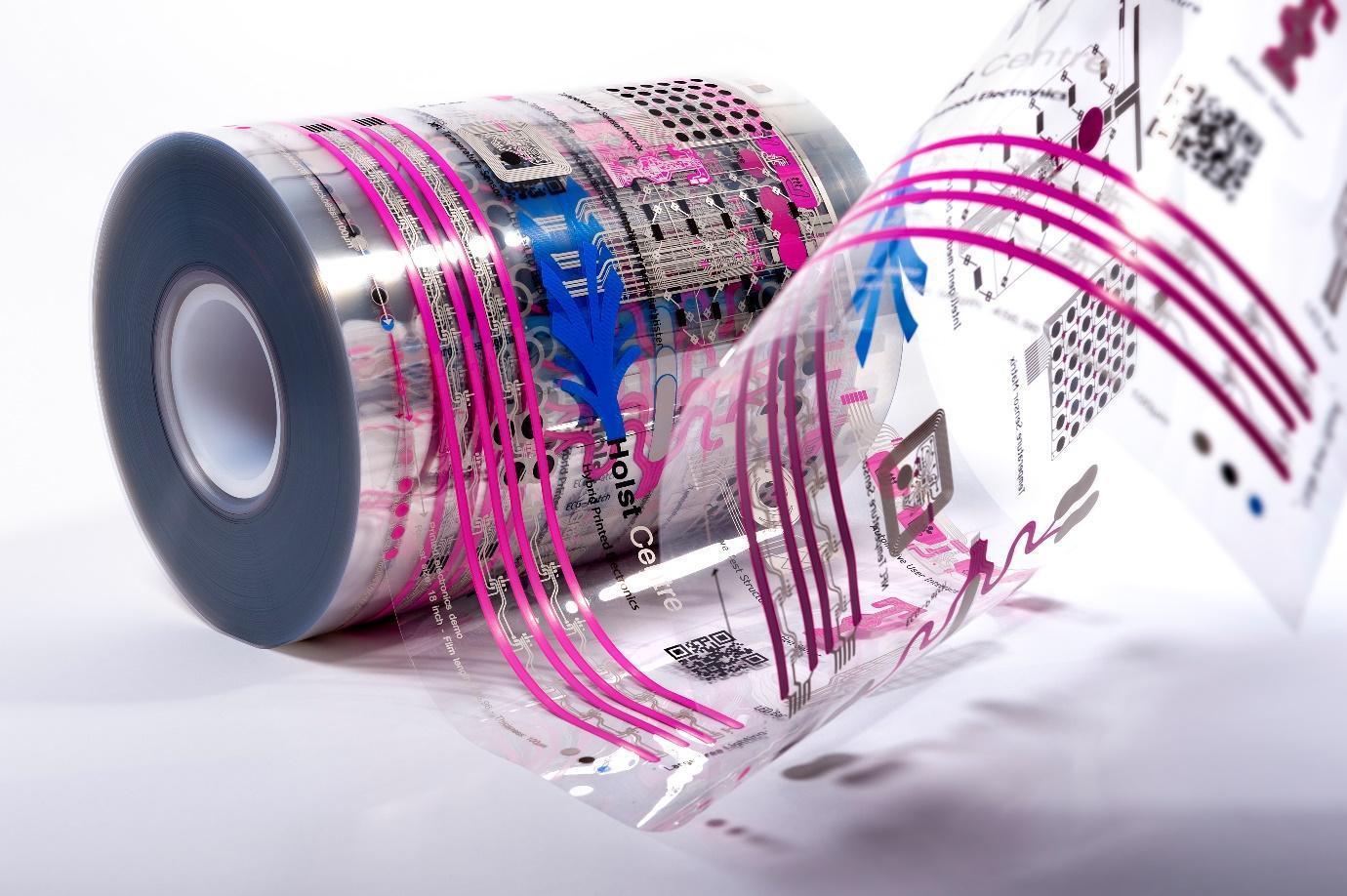
As a source of innovation in the Netherlands, Holst Centre has attracted attention both at home and abroad. It is a research and development organization whose core technology is printed and flexible electronics, which prints electronic circuits on thin, deformable films.
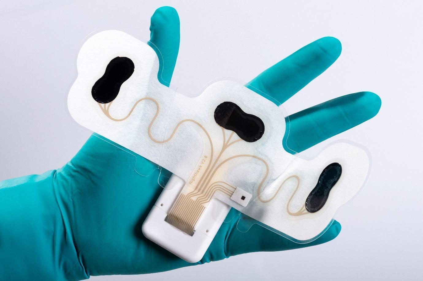
The institute has been particularly focused on remote medical technology, which is needed as the population ages. They have developed technologies for wearable devices that can be worn directly on the skin to automatically measure various vital signs from the comfort of your own home.
The next step for Holst Centre is the mass production of sustainable electronics of which the individual components can be recycled, as well as the development of advanced semiconductor packaging technologies and photonic chips that will support next-generation applications.
Holst Center's core competence is printed and flexible electronics technology. The institute's primary focus in areas where this technology is applied is in wearable medical devices.
With an aging population and a shortage of young medical professionals, the company aims to reduce the number of hospitalized patients and the burden on medical personnel by automating the measurement and monitoring of the various vital signs that is now done mostly manually and thus consumes a lot of time of health care staff.
Ton van Mol, Managing Director of the Holst Centre, explains,
“These devices will be especially needed in Japan, where the population is ageing. Our technology involves printing electronic circuits onto flexible thin films, making it ideal for application in wearables.
“But that is not the only advantage of printed electronics. PCBs (printed circuit boards) used in various conventional devices are wasteful, with processes of wet etching that wash away unneeded copper. In contrast, printed electronics add only what is needed, eliminating waste and reducing CO2 emissions by over 90% compared to PCBs.”
As a result of years of research and development in printed electronics, some start-ups were born at the Holst Centre. Those are TracXon, a foundry of hybrid printed electronics, FononTech, a new printing process equipment company, AIKON Health and Onera Health, medical data service providers using wearable devices.
“We are building a sustainable printed electronics value chain through these startups. We want to extend this to Japan and help Japanese companies transition from PCBs to sustainable electronics technology. We have already established a strategic partnership with Yamagata University and are encouraging Japanese companies to collaborate with us,” said van Mol.
The next step for the centre is to make products fully recyclable and circular.
“At the laboratory level, we can make electronic products that are completely recyclable. What we need to do next is to manufacture them and bring them to the market. To do this, we need to work with Japanese companies on materials development and set up a whole value chain.” (van Mol)
In addition to circular printed electronics, Holst Centre is also working on developing advanced semiconductor packaging and mounting technology to support next-generation applications.
“Our goal is to develop advanced semiconductor packaging, using printing technology. By stacking semiconductor chips vertically, many functions, such as antennas, can be placed in a smaller space, enabling smaller devices and improved performance. Also, circuits within a chip are placed closer to each other, reducing signal delays, power consumption, and cost,” says van Mol.
These technologies are expected to significantly improve device performance, especially in applications that process vast amounts of data, such as AI.

The Holst Center's vision of next-generation technology also extends to photonic chips. These chips use photons in addition to electrons to sense, process, and transmit data with unprecedented speed and sensitivity.
It is expected to be a key technology supporting next-generation applications such as data communications of the AI-era, telemedicine, and automated driving, and the Netherlands has positioned the development of the photonic chip industry as a national strategy.
Research is currently being conducted toward mass production of photonic chips under the Photonics Integration Technology Center (PITC), which was jointly established by the TNO (Netherlands Organization for Applied Scientific Research), Holst Centre, Eindhoven University of Technology, and the University of Twente, together with PhotonDelta, a network organization established based on a national fund. The Holst Centre also collaborates with PITC to create technology roadmaps, etc.
“Photonic chips will be essential for applications in the next 5-10 years. For example, the Holst Centre would like to develop a technology that would allow medical wearables to automatically measure not only vital signs such as heart rate and blood pressure, but also biochemicals in the blood such as glucose and bilirubin. If this becomes a reality, wearables could also be used to detect cancer in its early stages.”
According to van Mol, collaboration with Japanese industry is essential to this new endeavour.
“We sincerely welcome the cooperation of the Japanese people, who have very valuable technologies to realize our vision of a sustainable and healthy future,” he said.
Contact: Holst Centre