Holst Centre: Leading the way in sustainable and flexible electronics
2 min read
22 8月 2025
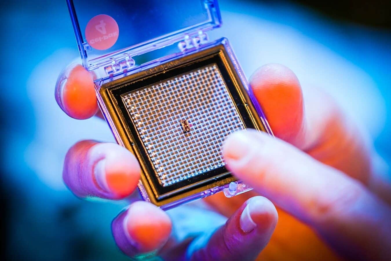
Holst Centre, a leading R&D hub in the Netherlands, is internationally recognised for its work in printed and flexible electronics – a technology that involves printing circuits onto thin, bendable films. These innovations are central to the development of sustainable devices and next-generation chips, particularly for healthcare systems facing pressure from aging populations like Japan’s.
Ton van Mol, Managing Director of Holst Centre and General Manager of the Photonics Integration Technology Center (PITC), explains how the organisation is shaping the future of electronics through collaboration, sustainability, and innovation.
This interview is based on a presentation at the Brabant Innovation Day 2024.

Holst Centre is known for its work in printed and flexible electronics. Why is this important, especially for ageing populations like Japan’s? What are the environmental advantages?
Printed electronics are ideal for wearables, which will become increasingly important in ageing societies like Japan. Our technology allows circuits to be printed on thin, flexible films, making them lightweight and adaptable for medical use. Printed electronics offer major environmental benefits. Unlike traditional printed circuit boards (PCBs), which waste materials through wet etching, our process prints only what’s needed.
Holst Centre has a goal to make electronics fully recyclable. What’s the next step and how can Japanese companies get involved?
At the lab level, we’ve already developed fully recyclable products. The challenge now is to scale up and bring them to market. For that, we need to collaborate with Japanese companies – especially in materials development – and build a complete value chain. Through startups like TracXon and FononTech, we’re creating a sustainable ecosystem, and we hope to expand this to Japan.
You’re also working on advanced semiconductor packaging. What are the advantages, especially for AI applications?
We’re using printing technology to develop advanced chip packaging through vertical stacking. This makes devices smaller and more powerful, with reduced signal delay, energy use, and cost. It’s especially important for AI, where fast and efficient data processing is critical.
What about photonic chips? How do you see them shaping the future, especially in healthcare?
Photonic chips use light instead of electrons to transmit and process data – faster, more efficiently, and with greater sensitivity. In healthcare, they could enable wearables that measure not just heart rate and blood pressure, but also blood biochemicals like glucose or bilirubin. Someday, they might even detect early-stage cancer. Beyond healthcare, photonic chips will support AI, autonomous driving, and telemedicine.
Holst Centre has a partnership with Yamagata University. What’s your message to Japanese companies?
We’ve already started working closely with Yamagata University, and we’re eager to collaborate more broadly. Japanese companies have unique technologies that can help realise our shared vision of sustainable, high-performance electronics. We warmly welcome their cooperation.