When Japanese tech giant Dai Nippon Printing (DNP) chose High Tech Campus Eindhoven for its first R&D hub outside Japan, it marked a historic milestone for both the company and the Brabant region. For DNP, founded in 1876, it was a bold leap into global collaboration. For Brabant, it was a powerful endorsement of its growing reputation as a world-class high-tech ecosystem. And it all began with a single meeting at the Brabant Innovation Days (BID) in Tokyo in 2023.
During BID, Edwin Zonder of the Brabant Development Agency (BOM) met Tsuyoshi Hotta from DNP in a session facilitated by the Netherlands Foreign Investment Agency. “Mr. Hotta showed immediate interest in High Tech Campus Eindhoven,” Zonder recalls. “He wanted to know more about the ecosystem, and that was our signal to act.”
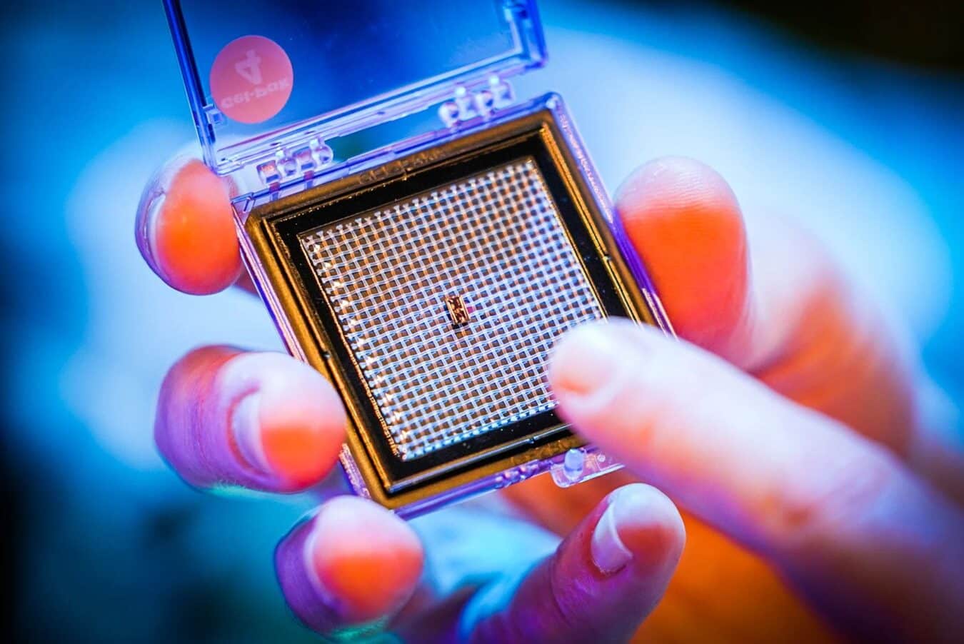
BID’s curated matchmaking approach is designed to turn introductions into real collaborations. And that initial conversation led to a fact-finding visit in July 2024, where DNP explored Brabant’s innovation landscape. The delegation toured Holst Centre labs, cleanrooms at High Tech Campus Eindhoven, and TU/e. “When we visited the cleanrooms, we immediately felt a strong connection with DNP’s technology,” said Koichi Suzuki, who will lead the new research base. “As the saying goes: seeing is believing.”
The visit confirmed what Mr. Hotta had sensed in Tokyo: Brabant offers a unique ecosystem of knowledge institutions, companies, and facilities recognised worldwide. “It’s the ideal place to develop new technology and collaborate with world leaders in photonics and semiconductors,” he says.
BOM remained closely involved, introducing DNP to potential partners. One quickly stood out: Holst Centre, a joint innovation initiative by TNO and imec. “The combination of TNO’s experience in applied research and system integration with DNP’s expertise in microfabrication and precision coating is extremely valuable,” says Hotta.
Together, they launched a joint R&D hub at Holst Centre, collaborating with the Photonic Integration Technology Centre (PITC) on a three-year programme.
This international collaboration not only strengthens Brabant’s position in semiconductors and photonics but also supports local institutions in addressing technological and societal challenges. “The fact that more Japanese companies are setting up R&D facilities here is a huge step,” says Zonder. “The presence of companies like DNP reinforces our entire ecosystem.” From one meeting in Tokyo to a groundbreaking partnership in Eindhoven, the DNP-BOM story is BID’s mission in action: to connect, collaborate, and co-create.