From promise to production: scaling photonic chips
At the point where photonic chip production meets industrial reality, Johan Feenstra, CEO of SMART Photonics, and Henk Akkermans, Professor of Supply Chain Management at Tilburg University, explore how production maturity is achieved in practice.
The technology to make photonic chips is there. This is no longer a distant promise: integrated photonics is moving into manufacturing and deployment right now. Rather than new breakthroughs, scaling now depends on three things: experience, effective and rapid feedback loops, and close cooperation across the ecosystem – a model that has been deliberately built in the Brabant region.
The next step is scaling production to industrial levels. Eindhoven, at the heart of the Brabant high-tech ecosystem, is home to SMART Photonics, a leading foundry for Indium Phosphide (InP) integrated photonic chips, which is at the forefront of this development. It has the experience and expertise to shift production to bigger wafers, enhancing yields and performance. “However, one thing is certain: we can’t do this alone”, CEO Johan Feenstra says.

We need the entire ecosystem to cooperate to make scaling photonic chip production a success.
Johan Feenstra, CEO SMART Photonics
Founded in 2012, in cooperation with the Technical University of Eindhoven (TU/e), SMART Photonics has been producing and selling photonic chips on a commercial basis for several years. It initially produced indium phosphide photonic chips on 2-inch wafers, before first switching to 3-inch and then 4-inch wafers in 2023. Now the company, supported by the Dutch government, the EU, and private investors, is ready for the next step: developing a new photonic chip production line, together with TNO, using 6-inch indium phosphide wafers. In Brabant, that scaling effort sits within a broader, world-class ecosystem that combines design capability, pilot lines and manufacturing readiness in a tightly connected region.
450 steps
The underlying photonic chip technology has been developing for decades, starting with fundamental research in the 1990s and progressing into applied research and early commercial use. Ramping up the production of photonic chips is required to meet growing demand – particularly driven by AI‑related datacom and high‑performance computing.
To speed up the scaling of photonics, several Dutch research organisations, including TNO (the Netherlands Organisation for Applied Scientific Research), established the Photonic Integration Technology Centre (PITC). As a joint, open R&D and innovation centre, PITC will be playing a crucial role in the development of the 6-inch photonic fab, in line with its mission to bridge the gap between advanced photonic chip research and practical applications. PITC partner TNO, together with High Tech Campus Eindhoven, is constructing what is described as the world’s first industrial factory for InP photonic chips on a 6-inch wafer scale. The pilot facility will be hosted at TNO’s Holst Centre and SMART Photonics is planning to invest in its own 6-inch wafer InP wafer production line – a step that highlights the growing focus on scaling production from research into industrial reality.
At this stage, however, scaling is less about new technological breakthroughs and more about execution. Successful scaling depends on fine-tuning processes, and applying top-notch engineering expertise and experience, according to Feenstra. “Our team has extensive experience in scaling photonics and growing the wafer size. It knows what issues to look out for and how to resolve them. Yet, we can’t do it alone.
Past experience with scaling of electronic semiconductor production demonstrated that cooperation within the ecosystem was crucial for its success. The same is true for photonics.
Johan Feenstra, CEO SMART Photonics
For instance, scaling requires collaboration with top-quality indium phosphide wafer suppliers, of which some of the best are located in Japan. “We are keen to work with them to develop the right specifics of new InP wafers,” Feenstra points out. SMART Photonics is also keen to tap into Japan’s expertise in the field of system integration. As photonics shifts from pilot capacity towards volume manufacturing, that creates timely opportunities for Japanese partners to collaborate on materials, equipment, integration and reliability.
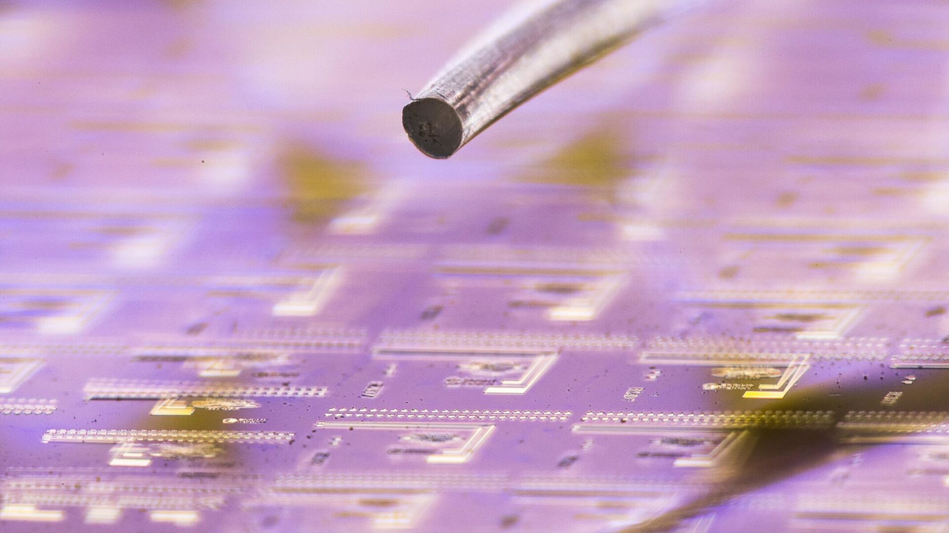
Producing a wafer with highly integrated photonic chips requires around 450 complex steps and takes three to four months to complete. Ramping up production means optimising each of these steps. The challenge of ensuring that all chips on a wafer function flawlessly becomes greater as the wafer size increases. A lot hinges on finding the right settings.
“When depositing a layer on a wafer using plasma deposition, for instance, a specific voltage is applied to the wafer,” says Feenstra. “This voltage determines the speed at which molecules are pulled to the wafer to create a layer of plasma. The challenge is to find the optimal voltage level. Spreading the layer equally over the wafer is another challenge. One needs a keen sense of touch for that – something our engineers have developed over the years.”
Collecting data for scaling
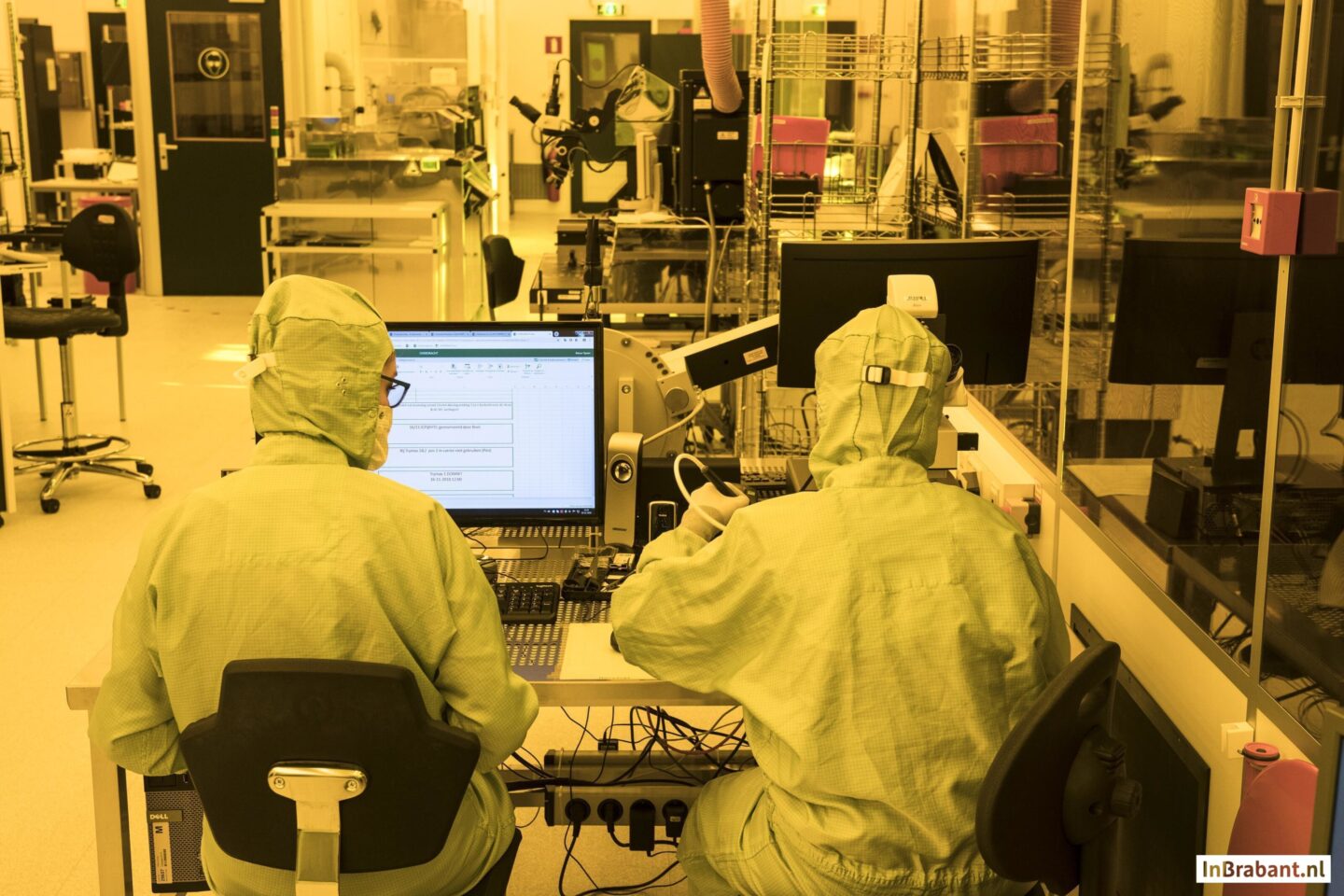
To improve the production processes and enhance the reliability of chip quality, SMART Photonics collects data during its different production steps. Data help identify where and how things go wrong and how improvements can be made.
“Developing effective feedback loops is exactly what should be done to scale high-tech production processes,” says Henk Akkermans, professor at Tilburg University and a researcher of supply-chain management.

Identifying the failure mode of a production process requires collecting data. No data, no learning, no improvement.
Henk Akkermans, professor at Tilburg University and a researcher of supply-chain management
“To be precise: collecting failure data is crucial. When did a component or process fail? How did it fail? And, very importantly, what was happening in the surrounding processes and components beforehand? With that understanding, our AI models can identify the ‘fingerprint’ of a failure mode. This shifts us from reacting to failures to anticipating them, enabling predictive maintenance. And when failures happen too often, it becomes a clear signal to redesign the component or process – in other words, to ‘design for maintenance’.
“Surprisingly, awareness about the need to collect performance data is often lagging,” adds Akkermans. Feedback loops are crucial, not only to improve the production process to higher scales and pace, but also to enhance product reliability. “This is true for any industrial production process and certainly for high-tech,” he says. “You never get it right the first time. This is why testing and metrology, collecting and analysing data are so important.”
His advice to the photonics industry: take the entire product life cycle into account from the start when designing a feedback system. “Such a system should be set up in a way that everyone working with the product feeds errors and results back downstream into the supply chain, including, for example, the suppliers of components for a production machine”, Akkermans explains. “Ideally, you figure out in close cooperation with partners what needs to be done to bring about improvements. To achieve reliability, it is not acceptable for a supplier to say, ‘Well, I’ve delivered and now I’m done’. No, that’s when it really begins.”
In pilot lines, those feedback loops become increasingly more predictive – using advanced analytics and AI to spot drift earlier, reduce variability, and improve yield and reliability over time.
10,000 wafers per year
The impact of photonic chips, which use light instead of electrons to perform calculations or transmit data, goes beyond commercial interests. The photonics industry as such has significant potential for positive societal impact, experts say. For example, photonic sensor chips can provide major advances in preventive medicine. Use of photonic chips could significantly reduce the energy consumption of data centres. Feenstra estimates this reduction at 20-25%.
Upon completion in 2028, the 6-inch pilot line is expected to produce around 10,000 wafers per year, corresponding to millions of photonic chips.
The pilot line will be hosted by TNO and is being built at the High Tech Campus in Eindhoven. It is part of the EU’s PIXEurope project. It marks an important step in demonstrating industrial-scale production – and shows how, in Brabant, scaling is driven not only driven by technology, but by the experience, feedback loops and ecosystem cooperation behind it. For partners in Japan, the shift to volume production creates a clear opportunity to collaborate more closely – particularly in areas such as materials, equipment and system integration – as the industry moves from capability to large-scale application.